You are here: Foswiki>QED Web>QedProjects>Cecile2ndDippingAt4K (07 Apr 2010, CecileHeraudeau)Edit Attach
Cecile2ndDippingAt4K
2nd dipping at 4K in the HelioxResonance at Room Temperature
2T Measurements
Use of the sensitive power supply : 100 micro Volts, 10 nA 4-6 : 5,5 nA 4-12 : 9,5 nA 4-13 : 9,8 nA 4-18 : 9,9 nA 4-16 : 0,4 nA Remarks : Pin 16 broken, again!4T Measurements
Use of the AC Lock-in Amplifier : 10 nA (1V through a 100MOhm transformer), 17 Hz of current excitation in Pin 4 13 - 16 : 41 (In) -2 (Out) 12 - 8 : 34 (In) -2 (Out) 12 - 13 : 0 (In) 0 (Out) 8 - 16 : 77 (In) -2 (Out) All results in micro Volts.I/Vg - Characterisitc
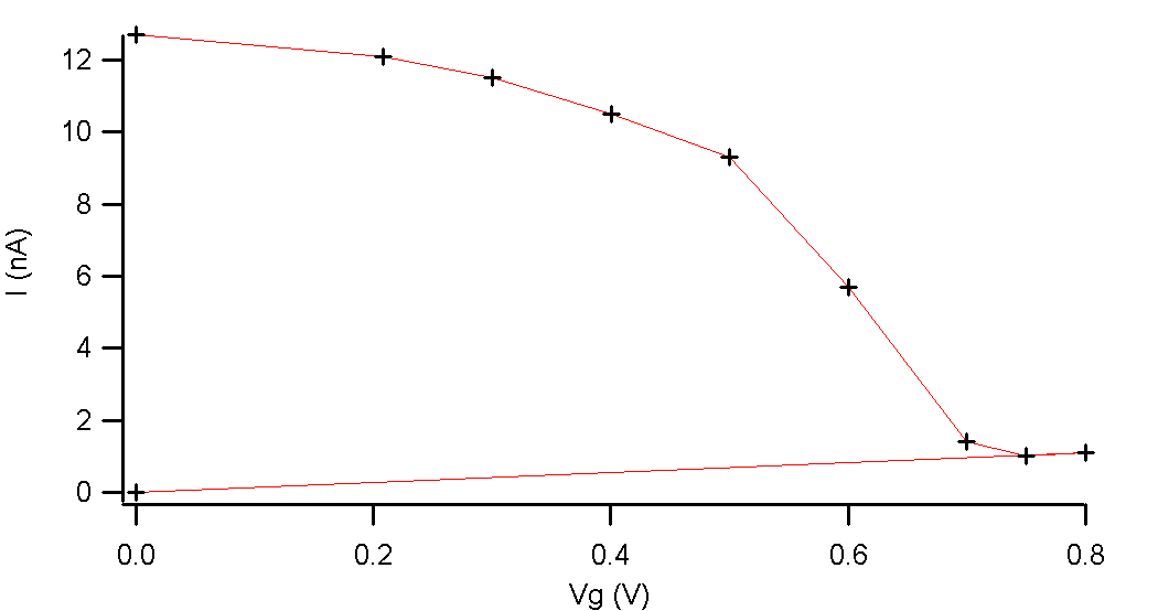
Use of 2 Lock-in amplifiers synchronized : 500 micro Volts (voltage attenuator) 17 Hz excitation -> Problem : we can't get a complete depletion (I=0V) of the device. Gate voltages used too high regarding to previous data.
Transfer function
Same parameters than for the IV characteristic The value of the resonant frequency is 350MH. TransferFunction.txt -> Problem: the measures doesn't seem rational, fluctuations in the resonance depth. Explanation? After ungrounded all the pins, new experimentsI/Vg - Characterisitc(2)
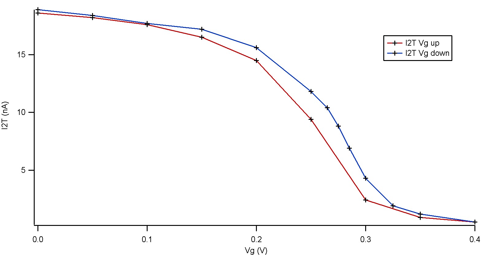
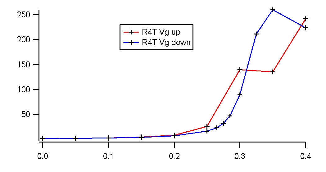
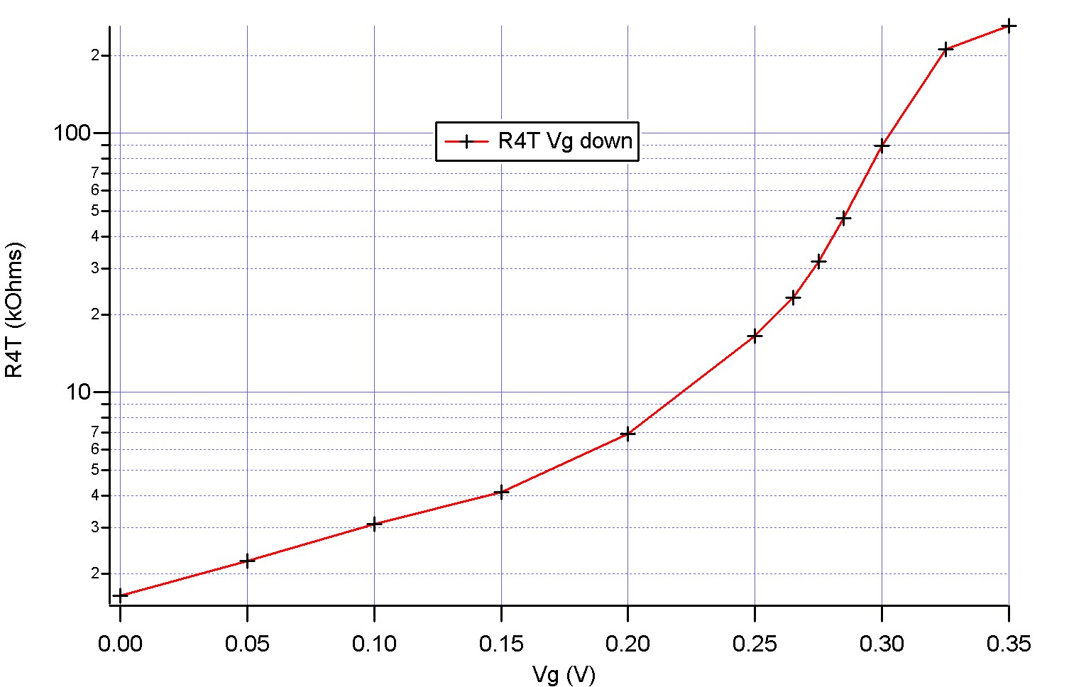
Procedure : 20 min at Vg=0V, then Vg Up 20 min at Vg=0.4V, then Vg down If we consider that the 4T resistance can be calculated as V4T/I2T (no current leakage to the ground or through the probes), then we can easily get this graph :
 The two last points (400 mV) are unrealistic.
If we compare this graph to Ben's work, we found it very similar, except for Vg up, where I apparently lack some data, and one point is probably false (0,350 mV).
Here is what I get :

RF Data (2)
After waiting 20 minutes at Vg=0.4VPCB Board
Tags
Comments
| I | Attachment | Action | Size | Date | Who | Comment |
|---|---|---|---|---|---|---|
| |
IVgCharacteristic2.bmp | manage | 2 MB | 30 Mar 2010 - 04:32 | CecileHeraudeau | |
| |
IVgcharacteristic3.jpg | manage | 80 K | 31 Mar 2010 - 04:56 | CecileHeraudeau | |
| |
PCB.JPG | manage | 1 MB | 01 Apr 2010 - 05:51 | CecileHeraudeau | |
| |
R4TvsVg.jpg | manage | 48 K | 31 Mar 2010 - 05:49 | CecileHeraudeau | |
| |
R4TvsVgLog.jpg | manage | 203 K | 31 Mar 2010 - 06:05 | CecileHeraudeau | |
| |
RES4.GIF | manage | 5 K | 30 Mar 2010 - 04:16 | CecileHeraudeau | |
| |
RES5.GIF | manage | 5 K | 30 Mar 2010 - 04:16 | CecileHeraudeau | |
| |
RES7.GIF | manage | 6 K | 31 Mar 2010 - 06:13 | CecileHeraudeau | |
| |
RES7.TIF | manage | 16 K | 31 Mar 2010 - 06:12 | CecileHeraudeau | |
| |
RES8.GIF | manage | 5 K | 31 Mar 2010 - 06:13 | CecileHeraudeau | |
| |
RES8.TIF | manage | 15 K | 31 Mar 2010 - 06:12 | CecileHeraudeau | |
| |
TransferFunction.txt | manage | 162 bytes | 30 Mar 2010 - 04:41 | CecileHeraudeau |
Edit | Attach | Print version | History: r4 < r3 < r2 < r1 | Backlinks | View wiki text | Edit wiki text | More topic actions
Topic revision: r4 - 07 Apr 2010, CecileHeraudeau
 Copyright © by the contributing authors. All material on this collaboration platform is the property of the contributing authors.
 Ideas, requests, problems regarding Foswiki? Send feedback


