|
|
You are here: Foswiki>QED Web>QedLabStuff>ResistS1813 (12 Feb 2010, SebastianFricke)Edit Attach
ResistS1813
Hints for using positive photoresist S1813.QPC measurements for chip prepared with resist S1813
Very high pinch-off voltage for exp_QPC_3_2 done by SebastianFricke in Dec. 2009. I prepared a QPC sample on a Cambridge A2900 wafer and for processing the hall bar ohmics and gates I used positive photoresist S1813. The QPCs were written with the Sirion EBL system. The outcome of the experiment conducted on the Heliox was, that one QPC on the sample that held 4 QPCs pinched off, but the pinch-off occurred at a very high voltage.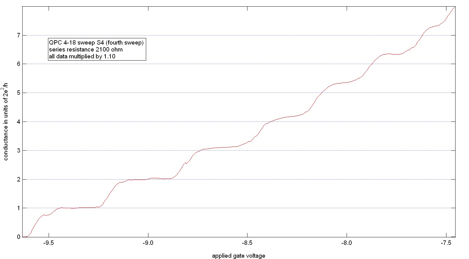 As visible in the graph above the QPC pinched off at a gate voltage of about -9.6. When you compare this value to the values in the literature, it is very high (in the literature the pinch-off voltages are ranging from -0.8V to about -2V). A possible expalnation for this very high pinch-off voltage might be the fact that the gates are not continous and that the electrons therefore have to tunnel through a tunnel junction. To investigate this we cleaved the chip in half across the hall bar and stuck it vertically onto a SEM stage.
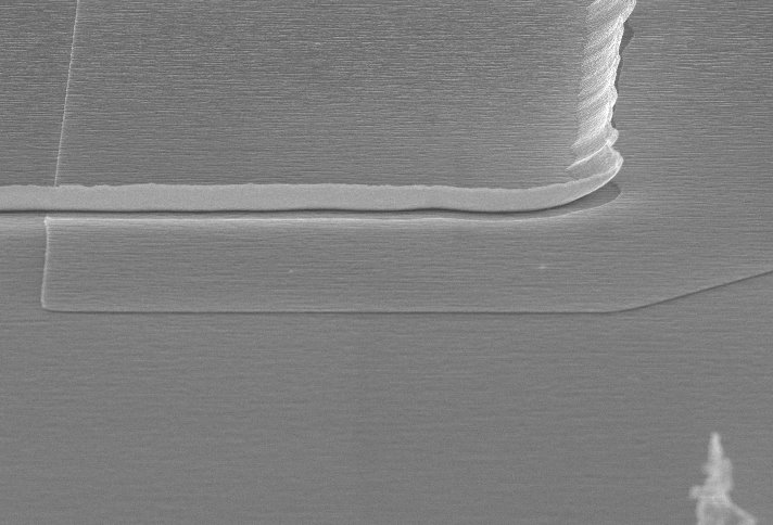
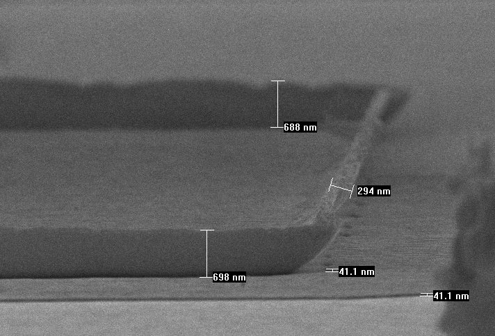
 As you can see in the pictures above, the metal is sticking roughly 700 nm up at the edges of the photolithographically defined metal gate and the thin EBL gate (thickness ~ 40 nm) can not overcome this huge rise of gate metal sticking upwards. This results in a gap between the photolithographically defined gate and the EBL gate. This gap is running all along the edge of the thick metal gate and therefore there is no direct electrical contact between the two gates which results in a tunnel junction and explains the high pinch-off voltages I got in my experiment of exp_QPC_3_2.
The reason for the metal gate sticking upwards is the resist profile of positive resist S1813. Instead of getting a clear undercut, the resist is hardened at the top due to the chlorobenzene soak and you get a slight undercut, but then the positive resist profile is sloping outwards and metal will be deposited on this slope and stay tilted upwards when the resist is washed away. The following SEM picture might show this a little bit more clearly.
As you can see in the pictures above, the metal is sticking roughly 700 nm up at the edges of the photolithographically defined metal gate and the thin EBL gate (thickness ~ 40 nm) can not overcome this huge rise of gate metal sticking upwards. This results in a gap between the photolithographically defined gate and the EBL gate. This gap is running all along the edge of the thick metal gate and therefore there is no direct electrical contact between the two gates which results in a tunnel junction and explains the high pinch-off voltages I got in my experiment of exp_QPC_3_2.
The reason for the metal gate sticking upwards is the resist profile of positive resist S1813. Instead of getting a clear undercut, the resist is hardened at the top due to the chlorobenzene soak and you get a slight undercut, but then the positive resist profile is sloping outwards and metal will be deposited on this slope and stay tilted upwards when the resist is washed away. The following SEM picture might show this a little bit more clearly.
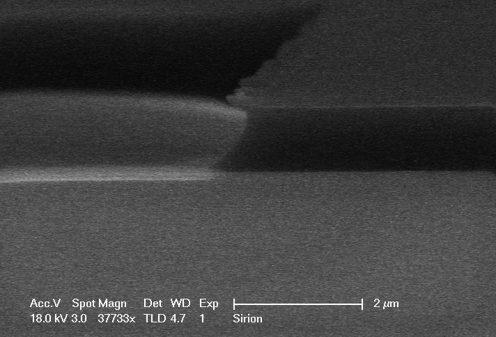
 You can see at the bottom of the resist that HF has etched underneath the resist. But the resist profile does not show a clear undercut. This will lead to the observed metal edges of the gate.
Tags
Comments


| I | Attachment | Action | Size | Date | Who | Comment |
|---|---|---|---|---|---|---|
| |
250110_1.jpg | manage | 58 K | 12 Feb 2010 - 04:47 | SebastianFricke | |
| |
250110_6.jpg | manage | 85 K | 12 Feb 2010 - 04:48 | SebastianFricke | |
| |
Conductance_QPC_4_18_LED_S4_corr.jpg | manage | 105 K | 12 Feb 2010 - 04:32 | SebastianFricke | |
| |
HF3.jpg | manage | 75 K | 12 Feb 2010 - 05:00 | SebastianFricke |
Edit | Attach | Print version | History: r1 | Backlinks | View wiki text | Edit wiki text | More topic actions
Topic revision: r1 - 12 Feb 2010, SebastianFricke


Ideas, requests, problems regarding Foswiki? Send feedback