You are here: Foswiki>QED Web>QedLabStuff>WaferLog>WaferW1557 (23 Sep 2020, AlexHamilton)Edit Attach
Wafer1557
Wafer from Cambridge. Received on 15/01/2020 This is an induced wafer.Growth details
Here is a scan of the MBE growth sheet: W1557_Growth_sheet.pdf Essentially the growth is:| GaAs | - | 2nm |
| AlGaAs | - | 33nm |
| GaAs | - | 1um |
Characterisation details
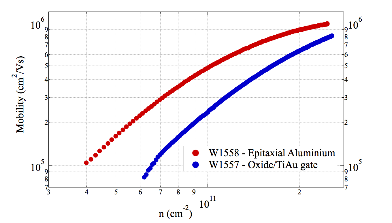
Here are characterisation data from the MBE growers (if available) - (insert scanned jpg here). Here are some of our own characterisation data (insert jpg & details of measurement T, date, by whom, file location) T = 0.25K, Processed and measured by Yoni
 smb://infpwfs605.ad.unsw.edu.au/PHY/researchgroups/gqed/Yonatan/PhD/PhD Work/Projects/Epitaxial Aluminium/Cambridge/W15 batch/Comparison/Density.jpg
Different colours are different gate voltages:
 smb://infpwfs605.ad.unsw.edu.au/PHY/researchgroups/gqed/Yonatan/PhD/PhD Work/Projects/Epitaxial Aluminium/Cambridge/W15 batch/W1557/Measurements/SdH/SdHC - A3.2 RUN 2/SdHCAll.jpg
Material usage
Here is a scanned copy of the wafer usage sheet from the measurement lab. This should be updated regularly by whoever takes a piece of wafer.Processing hints / tips
Please give details of processing that worked well for this wafer. Even a scan of a lab-book page, with details of contact resistances etc.| I | Attachment | Action | Size | Date | Who | Comment |
|---|---|---|---|---|---|---|
| |
Density.jpg | manage | 512 K | 29 May 2020 - 23:47 | YonatanAshlea | |
| |
Mobility.jpg | manage | 406 K | 29 May 2020 - 23:44 | YonatanAshlea | |
| |
SdHCAll.jpg | manage | 1 MB | 29 May 2020 - 23:50 | YonatanAshlea | |
| |
W1557_Growth_sheet.pdf | manage | 36 K | 29 May 2020 - 23:36 | YonatanAshlea |
Edit | Attach | Print version | History: r2 < r1 | Backlinks | View wiki text | Edit wiki text | More topic actions
Topic revision: r2 - 23 Sep 2020, AlexHamilton
 Copyright © by the contributing authors. All material on this collaboration platform is the property of the contributing authors.
 Ideas, requests, problems regarding Foswiki? Send feedback


