| |
Quantum Electronic
Devices
@ UNSW |
Current Research
Researchers within the QED group are investigating the electrical properties of novel 2D materials and nanometer scale semiconductor devices. In these materials the device properties are no longer governed by semi-classical physics, but are instead determined by quantum mechanical effects. The group makes its own quantum semiconductor devices here at UNSW, and uses a variety of electronic probes at milliKelvin temperatures and in strong magnetic fields to further the understanding of quantum electronics: 1. Using valence band holes in nanostructure devices for spin qubits and quantum device applications.It has been known for over 100 years that electricity is semiconductors is carried by negatively charged electrons and positively charged holes. However while the properties of electrons are very well understood, the understanding of holes (particularly when confined to move in nanostructures) is much less well understood. For example, you have probably been taught that valence band holes are essentially just heavy electrons, with a positive charge and a positive effective mass. This is incorrect. Holes are spin-3/2 particles whereas electrons are spin-1/2. It is only in the past few years that we are beginning to understand just how different holes are from electrons. For instance, whereas electrons have a well defined dipole moment that couples their spin to an externally applied magnetic field, holes also have quadrupole and octopole moments that have no equivalent in electrons. These unique spin properties have led to proposals for novel spin based hole transistors, that could run much faster and with lower power than conventional devices that rely on the charge of electrons, as well as new types of quantum bits for quantum information applications. 2. Artificial Quantum Matter: Nanopatterned semiconductor devices to create artificial bandstructures
Oleh Klochan is leading a project to create devices with new electronic and magnetic properties that are determined by a nanoscale artificial surface superlattice, rather than by the host semiconductor material. 3. Hydrodynamic flow of electrical currents in transistors
Hydrodynamics (how fluids move) governs the motion of matter ranging from sub-atomic length scales (the quark-gluon plasma) to everyday length scales (how air moves around cars and airplanes) out to cosmological length scales (how galaxies move). But although the equations governing fluid flow have been well known for over 100 years, much is not understood - for example there is no universal theory of turbulence. In high quality two dimensional transistors electrons can flow like a fluid - which provides a new platform for exploring the properties of classical and quantum fluids. Current projects:
  |
Hole spin qubits in silicon and germanium quantum dots Although there has been much work studying electrons in silicon and SiGe quantum dots, there has been much less work on holes in silicon and germanium quantum dots. Unlike electrons in silicon, holes have a strong spinorbit interaction and are very interesting for the study of spin control and manipulation using only electric fields. In collaboration with the IMEC consortium in Europe, Andrew Dzurak's group in ANFF, and Giordanno Scappucci and Menno Veldhorst at TUDelft, we are studying the properties of holes in silicon MOS quantum dots and Ge heterostructure quantum dots. SD Liles, et al, A singlet-triplet hole-spin qubit in MOS silicon, Nature Communications 15, 7690 (2024) https://doi.org/10.1038/s41467-024-51902-9 I. K. Jin et al, Combining n-MOS Charge Sensing with p-MOS Silicon Hole Double Quantum Dots in a CMOS platform , Nano Lett. 23, 1261–1266 (2023). LA Terrazos, E Marcellina, Z. Wang, SN Coppersmith, M. Friesen, AR Hamilton, X. Hu, B. Koiller, AL Saraiva, D. Culcer, RB Capaz, Theory of hole-spin qubits in strained germanium quantum dots, Physical Review B 103, 125201 (2021). S. D. Liles, R. Li, C. H. Yang, F. E. Hudson, M. Veldhorst, A. S. Dzurak, and A. R. Hamilton, Spin and orbital structure of the first six holes in a silicon metal-oxide-semiconductor quantum dot, Nature Communications 9, 3255 (2018) R. Li, F. E. Hudson, A. S. Dzurak, and A. R. Hamilton, Single hole transport in a silicon metal-oxide-semiconductor quantum dot, Appl. Phys. Lett. 103, 163508 (2013). |
 |
Artificial Quantum Matter: Making designer electronic bandstructures from conventional semiconductors Working in collaboration with Oleh Klochan's group we are developing 2D materials whose electronic properties are determined by a electron beam lithography patterned surface superlattice, instead of the semiconductor itself. This opens a new route to making artificial graphene and topological insulators from conventional materials such as silicon, as well as enabling the study of new electronic phases in 2D materials. D. Q. Wang et al., Formation of Artificial Fermi Surfaces with a Triangular Superlattice on a Conventional Two-Dimensional Electron Gas , Nano Letters 23, 1705 (2023). See also: M. Polini, F. Guinea, M. Lewenstein, H. C. Manoharan, and V. Pellegrini, Artificial honeycomb lattices for electrons, atoms and photons , Nature Nanotechnology 8, 625–633 (2013). |
 |
Hydrodynamic flow of electrical currents in transistors Hydrodynamics (how fluids move) govens the motion of matter ranging from sub-atomic length scales (the quark-gluon plasma) to everyday length scales (how air moves around cars and airplanes) out to cosmological length scales (how galaxies move). But although the equations governing fluid flow have been well known for over 100 years, much is not understood - for example there is no universal theory of turbulence. In high quality two dimensional transistors electrons can flow like a fluid that’s two hundred times thicker than honey. This is certainly not what we expect from undergraduate physics! The textbook theory for electron conduction—the Drude model—describes a solid as a pinball machine, with the electrons bouncing off the atoms in the crystal lattice. But a more detailed theory predicts the possibility of an exotic regime in which the electrons flow through a solid and interact with each other like molecules in a viscous fluid. This fluid-like behavior could be harnessed in novel electronic devices and in experiments that mimic other fluid systems. To reach this regime, the temperature should be so low that electrons are unlikely to scatter from thermally excited crystal vibrations and the material so pure that the scattering of electrons off defects is rare. We have developed new types of 2D quantum transistors based on compound semiconductors, as well as devices based on graphene, in which this hydrodynamic flow can be studied over a wide range of temperatures. The hydrodynamic flow causes a deviation from Ohms law, and can be used to probe the validity of Fermi liquid theory. The aim of this project is to measure electron flow in these devices from -270C to room temperature, and look for signatures of hydrodynamic flow. A. C. Keser et al., Geometric Control of Universal Hydrodynamic Flow in a Two-Dimensional Electron Fluid , Phys. Rev. X 11, 031030 (2021). |
 |
In a very low disorder short one-dimensional quantum wire, electrons or holes can travel without scattering at low temperatures - they behave as waves rather than particles. While the spin properties of electrons in quantum wires are mostly well understood, there is not even a basic understanding of the spin properties of holes in quantum wires. This is a bit surprising given that the average computer chip contains billions of transistors based on hole quantun wires! For example, whereas the spin-splitting of electrons in a magnetic field is simply given by ΔE=gμ K. L. Hudson, A. Srinivasan, O. Goulko, J. Adam, Q. Wang, L. A. Yeoh, O. Klochan, I. Farrer, D. A. Ritchie, A. Ludwig, A. D. Wieck, J. von Delft & A. R. Hamilton, New signatures of the spin gap in quantum point contacts , Nature Communications 12, 5 (2021). A. Srinivasan, D. S. Miserev, K. L. Hudson, O. Klochan, K. Muraki, Y. Hirayama, D. Reuter, A. D. Wieck, O. P. Sushkov and A. R. Hamilton, Detection and control of spin-orbit interactions in a GaAs hole quantum point contact , Phys. Rev. Lett 118, 146801 (2017). J.C.H. Chen et al, Observation of orientation- and k-dependent Zeeman spin-splitting in hole quantum wires on (100)-oriented AlGaAs /GaAs Heterostructures, New Journal of Physics 12, 033043 (2010). |
 |
Hole spin qubits in gallium-arsenide quantum dots Hole spins in GaAs semiconductors have a strong spinorbit interaction and a weak hyperfine coupling to the surrounding nuclear spins, and therefore, are very interesting for the study of spin control and coherence times. D.Q. Wang, O. Klochan, J-T Hung, D. Culcer, I. Farrer, D.A. Ritchie, and A.R. Hamilton, Anisotropic Pauli Spin Blockade of Holes in a GaAs Double Quantum Dot , Nano Letters 16, 7685 (2016). D Q Wang, A R Hamilton, I Farrer, D A Ritchie and O Klochan, Double-layer-gate architecture for few-hole GaAs quantum dots, Nanotechnology 27, 334001 (2016). |
 |
Developing new materials for future quantum devices We are developing new ways to make ultra reliable quantum devices with new functionalities, by combining metals and semiconductors into single crystal structures: Y. Ashlea Alava, D. Q. Wang, C. Chen, D. A. Ritchie, O. Klochan, and A. R. Hamilton, High electron mobility and low noise quantum point contacts in an ultra-shallow all-epitaxial metal gate GaAs /AlxGa1−xAs heterostructure , Appl. Phys. Lett. 119, 063105 (2021). Highlighted as an Editor’s pick. Asbjørn C. C. Drachmann, Rosa E. Diaz, Candice Thomas, Henri J. Suominen, Alexander M. Whiticar, Antonio Fornieri, Sergei Gronin, Tiantian Wang, Geoffrey C. Gardner, Alex R. Hamilton, Fabrizio Nichele, Michael J. Manfra, Charles M. Marcus, Anodic Oxidation of Epitaxial Superconductor-Semiconductor Hybrids, Phys. Rev. Materials 5, 013805 (2021). A. Srinivasan, I. Farrer, D. A. Ritchie, and A. R. Hamilton, Improving reproducibility of quantum devices with completely undoped architectures , Appl. Phys. Lett. 117, 183101 (2020). H. J. Suominen, M. Kjaergaard, A. R. Hamilton, J. Shabani, C. J. Palmstrøm, C. M. Marcus, and F. Nichele, Zero-Energy Modes from Coalescing Andreev States in a Two-Dimensional Semiconductor-Superconductor Hybrid Platform, Physical Review Letters 119, 176805 (2017). |
 |
The electronic and magnetic properties of two-dimensional holes in semiconductor quantum wells We perform electrical measurements of hole based devices at ultra-low temperatures and in intense magnetic fields to understand their complex spin properties. E. Marcellina, A. Srinivasan, D. S. Miserev, A. F. Croxall, D. A. Ritchie, I. Farrer, O. P. Sushkov, Dimitrie Culcer, and A. R. Hamilton, Electrical Control of the Zeeman Spin Splitting in Two-Dimensional Hole Systems, Physical Review Letters 121, 077701 (2018). T Li, LA Yeoh, A Srinivasan, O Klochan, DA Ritchie, MY Simmons, OP Sushkov and AR Hamilton, Manifestation of a non-Abelian Berry phase in a p-type semiconductor system, Physical Review B 93, 205424 (2016). A. Srinivasan et al, Using a tuneable quantum wire to measure the large out-of-plane spin splitting of quasi two-dimensional holes in a GaAs nanostructure, Nano Letters 13, 148 (2013). |
|
|
Electronic properties of 2D topological materials The physical properties of materials are strongly related with their electronic and crystal structures. Tungsten ditelluride (WTe2) is in a class of materials known as transition metal dichalcogenicdes – they are layered materials in which the atoms within a layer are held together by strong covalent bonds, but the layers stick together by weak van der Waals forces. WTe2 is particularly interesting material – in it’s bulk form it is a semimetal, but a monolayer can be a (topological) insulator, a superconductor, or a conventional semiconductor. Recently we showed that WTe2 is also a (semi)-metallic ferroelectric – a very unusual state, since ferroelectricity usually only occurs in insulators. This is because the charge dipoles that cause ferroelectricity would normally be screened by conduction electrons. However scanning probe measurements of both bulk and thin film WTe2 have clearly shown ferroelectricity [1]. Another question is how does isolating a single sheet of WTe2 from a bulk crystal change it’s electronic properties? To answer this question we have used low temperature magnetotransport measurements in tilted magnetic fields to study the band structure evolution while systematically changing the sample thickness. [2]
|
|
|
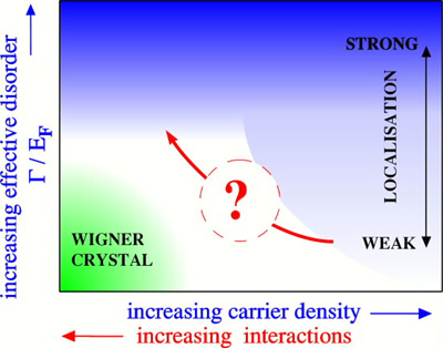
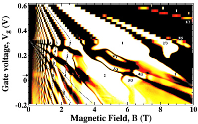
Electron-electron interactions and the forbidden metal-insulator transition in two dimensional systems Most transistors, such as the building block of modern computers, the MOSFET, use a thin (two-dimensional) sheet of highly mobile electrons to carry the electric current. These 2D systems are not only of immense technological significance, but have led to profound new fundamental phenomena, with discoveries such as the Quantum Hall Effect, the Fractional Quantum Hall Effect, and the High Electron Mobility Transistor (HEMT) have each leading to separate Nobel Prizes (1985, 1998, and 2000 respectively). However, despite being created over 40 years ago, there is still no universally accepted theoretical understanding of the fundamental electronic properties of high quality two-dimensional systems. Even the nature of the electronic state is not completely known over the complete range of carrier density and disorder (pictured left). |
|---|---|
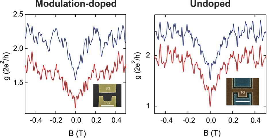 |
Undoped AlGaAs/GaAs Semiconductor Billiards Disorder increasingly affects performance as electronic devices are reduced in size. The ionized dopants used to populate a device with electrons lead to unpredictable changes in the behaviour of devices such as quantum dots each time they are cooled for use. We show that a quantum dot can be used as a highly sensitive probe of changes in disorder potential and that, by removing the ionized dopants and populating the dot electrostatically, its electronic properties become reproducible with high fidelity after thermal cycling to room temperature. Impact of Small-Angle Scattering on Ballistic Transport in Quantum Dots A. M. See, I. Pilgrim, B. C. Scannell, R. Montgomery, O. Klochan, A. M. Burke, M. Aagesen, P. E. Lindelof, I. Farrer, D. A. Ritchie, R. P. Taylor, A. R. Hamilton and A. P. Micolich, Phys. Rev. Lett., 108, 196807 (2012). |
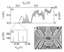 |
Single electron/hole transistors and quantum dots In a single electron transitor it is possible to observe effects associated with the motion of individual electrons. We have developed a novel technique for making highly stable nanoscale single electron and single hole transistors, and are investigating the coherent properties of electrons and holes in quantum dots and chaotic billiards. For further details see O. Klochan et al, Applied Physics Letters 96, 092103 (2010) and A.M. See et al, Applied Physics Letters 96, 112104 (2010).
|
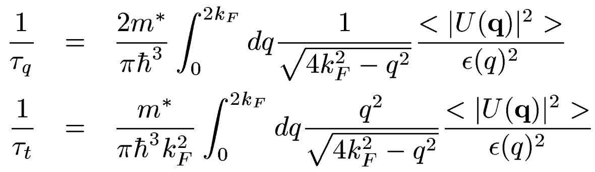 |
Quantum and scattering lifetimes in two dimensional systems We are examining the low-temperature properties of high-quality heterostructures, in which scattering is dominated by two types of disorder: remote ionised impurities (RII) and homogeneous background (BG) impurities. However it turns out calculations involving the homogeneous background impurities, which affect all quantum devices, is non-trivial and hinders direct comparison between theory and experiment. We are working to make comparison between theory and experiment easier, and to related these scattering lifetimes to observed transport phenomena. |
 |
Inter-device interactions in strongly coupled quantum devices As the dimensions of individual components in a "chip" shrink, and we pack these components ever closer together, it will no longer be possible to ignore interactions between devices. So as well as understanding how electron-electron interactions within a device affect its electrical properties, it is also important to understand the interactions between devices in order to design the next generation of nano-electronic devices. |